-40%
2x DIY PCB: A40 Class A Audio Power Amplifier
$ 5.26
- Description
- Size Guide
Description
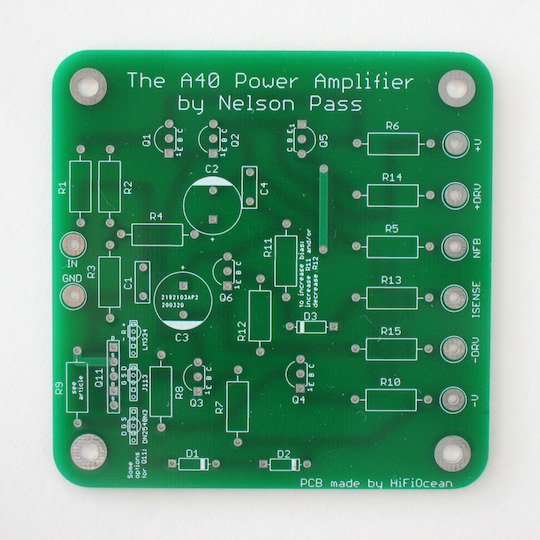
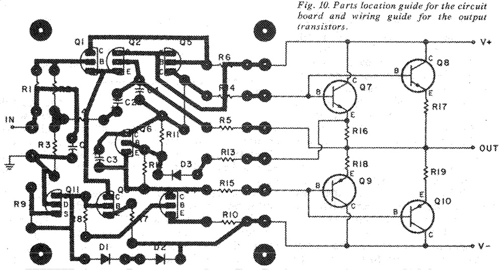
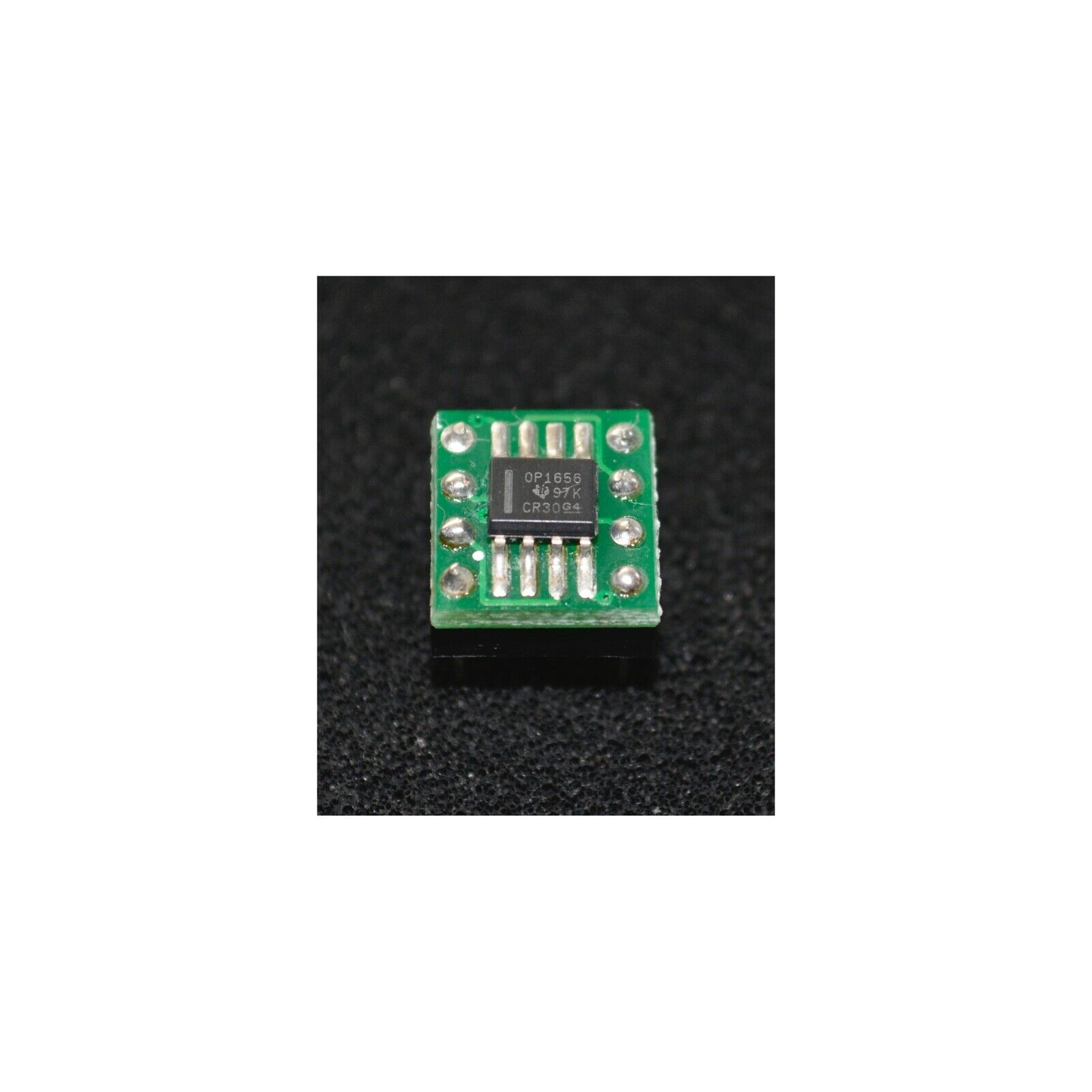
The A40 power amplifier is a 40 Watts per channel, Class A audio power amplifier design by Nelson Pass. Despite being around for more than 40 years, it has a steady following, with some people saying this is still one of the best sounding BJT audio power amplifiers around, especially upgraded to the newer transistors currently available.The PCB implements the front end for one channel. Two boards are required for a stereo amplifier. The output stage (4x power Darlinton transistors and 4x 0.68ohm emitter resistors) needs to be assembled off board. The board closely follows the published design with two exceptions: it is double sided and allows different pinouts for Q11, the JFET used as a current source.
Part substitution (based on the article by Nelson Pass):
The Lambda output devices specified in the BOM are no longer available. Common everyday complementary power darlington transistors will substitute for these. They need to be rated at 75 watts or higher, 5 amps or higher, and 80 volts or higher. Good examples of these are the TIP142 (NPN) and TIP147 (PNP). Another fine example are the MJ11012, MJ11014, and MJ11016 (NPN) and MJ11013 and MJ11015 (PNP).
The remaining bipolar transistors MPSL01 and MPSL51 can be substituted by ordinary TO-92 devices rated at voltages of 100 volts or more, and currents of 25 mA or more. For best results the beta (current gain) of the devices should be 100 or greater. Q3, Q4, and Q5 should be fitted with heat sinks, such as Aavid 575200B00000G (Mouser part number 532-575200B00).
It is possible that the bias might be at a slightly different value with these substitutions, in which slightly altering the values of R11 or R12 will allow some adjustment. A slight increase of R11 or decrease of R12 will increase the bias, and vice versa. The original article recommends biasing the amplifier at 1.5A of quiescent current.
The JFET in the circuit, Q11, is used as a constant current source to bias a few milliamps through D1 and D2 which provides a clean voltage reference for the constant current sources Q3 and Q4. You can substitute this part with another N channel JFET (e.g. J111/112/113) or a depletion mode MOSFET (e.g. DN2540) which has been tested to act as a current source in the circuit with R9; the board will accept parts with any pinout. The value of R9 needs to be chosen so that the JFET/MOSFET passes about 3 mA or so; the value is not critical. You can also substitute in a monolithic constant current source, rated at about this current and 40 volts, such as LM334. In this case, refer too the current source's datasheet to determine the value of R9. For LM334, the value of R9 should be between 22 and 33 ohms.
